From Node to Package: The Migration of the Compute Bottleneck
For a decade the Moore's Law narrative revolved around shrinking process nodes — from 7nm to 3nm to 2nm. But as per-chip transistor density approaches physical limits, the industry has found that what really governs AI accelerator performance and output is how logic dies, high-bandwidth memory (HBM) and silicon interposers are packaged together. TSMC's CoWoS (Chip-on-Wafer-on-Substrate) is shorthand for that step — and the scarcest capacity of 2026.
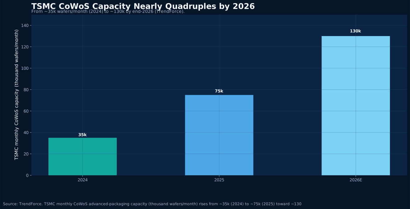
According to TrendForce tracking, TSMC's monthly CoWoS capacity has expanded from ~35k wafers in 2024 to ~75k in 2025 and is projected to reach ~130k by end-2026 — nearly quadrupling in two years. TSMC has said at its technology forum that CoWoS capacity will grow at a CAGR above 80% from 2022 to 2027, with 2026 packaging output roughly ten times that of 2023. The speed of the build-out itself testifies to the intensity of demand.
Chiplets: Breaking the Big Die into Building Blocks
The core idea of the chiplet architecture is to abandon fabricating one giant, expensive monolithic die and instead split functions — compute, I/O, memory control — into several smaller dies, then reassemble them with advanced packaging. This lifts yield, cuts cost and lets designers mix process nodes, reserving the most advanced process for the logic that truly needs it. For AI chips it is almost the only viable path to scale.
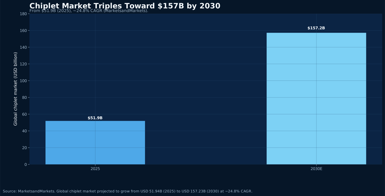
The market's confidence in this direction shows in the numbers. MarketsandMarkets estimates the global chiplet market will grow from $51.9B in 2025 to $157.2B in 2030 — roughly tripling in five years at a ~24.8% CAGR. That growth is driven almost entirely by AI training and inference and by high-performance computing, while packaging capacity is the physical constraint that turns design blueprints into deliverable product.
Locked-Up Demand: Nvidia and the Allocation Game
The scarcity of advanced packaging shows up most directly in customers' scramble for capacity. Multiple industry outlets report that Nvidia has reserved about 60% of TSMC's 2026 advanced-packaging capacity, much of it allocated to the newer CoWoS-L technology. When a single customer locks up more than half of supply, every other AI chip designer — cloud players building custom ASICs, or emerging accelerator startups — must queue for what remains.
To ease the bottleneck, TSMC is spilling some orders to OSAT (outsourced assembly and test) partners, with alternatives such as ASE's CoWoP drawing attention; TrendForce expects the CoWoS supply-demand gap to narrow from about 20% to roughly 10% by end-2026 as capacity comes online. Even so, advanced packaging will remain a seller's market for the foreseeable future — whoever secures capacity sets the launch cadence for AI servers.
HBM and Packaging: Korea's Pivotal Position
On the advanced-packaging value chain, Korea holds an irreplaceable position. Every CoWoS-packaged AI accelerator stacks multiple HBM dies, and global HBM supply is highly concentrated in SK Hynix and Samsung Electronics. In other words, packaging capacity expansion must move in lockstep with HBM output; a shortage at either end becomes the bottleneck for the whole system. That is why memory and packaging are jointly called the “twin engines” of AI compute.
At the same time, mainland China is doubling down on advanced packaging: industry reports put planned Chinese investments in chiplet and 3D integration and AI-chip substrate projects across several regions at hundreds of billions of yuan in 2026, aiming to break out via packaging where process nodes are constrained. For supply-chain players straddling China and Korea, the coordination of packaging, substrate and HBM capacity is reshaping the region's division of labor.
Implications for Sourcing and Supply Chains
For downstream server makers, device brands and system integrators, the tightness in advanced packaging means delivery-timing uncertainty is moving upstream. Previously chip lead times hinged mainly on the fab line; now, even if a logic die tapes out smoothly, failing to secure a packaging slot can push system delivery out by months. Buyers need to treat packaging capacity as a core supply-assurance metric, not just watch wafer capacity.
In helping China–Korea manufacturing and trade clients plan supply chains, MO-TEK recommends making “packaging availability” a precondition in negotiations for AI-related hardware procurement, and writing capacity reservations and alternative packaging options explicitly into contracts. For substrates and related materials, locking in capacity early and building multi-source supply will be key to stability through 2026–2027.
Outlook: Packaging as Strategy
Looking back from mid-2026, advanced packaging has been upgraded from a process step to the strategic link that decides the AI-hardware competitive landscape. Process nodes still advance, but as the marginal returns of 2nm and 1.4nm diminish while costs jump, efficiently integrating diverse chiplets in 2.5D and 3D becomes the most economical way to lift system performance. That means the center of gravity of industry investment will keep tilting for years from pure wafer lines toward back-end links — packaging, substrates and test — with related equipment and materials suppliers seeing structural demand expansion.
For firms on the China–Korea supply chain, the lesson is clear: rather than watching only who can build the most advanced logic die, also watch who can provide packaging capacity, substrate materials, test services and consumables. The technical barriers of these links may be lower than the leading node, yet they carry considerable commercial value thanks to firm demand and rapid ramp. MO-TEK will keep tracking the capacity and price signals along this chain, helping clients find grounded, capability-matched ways to participate in the AI-hardware wave.